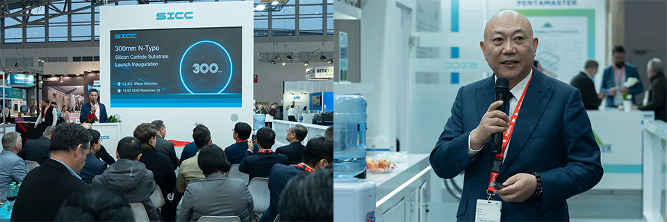
The Electronica Show and Semicon Europa will take place in Munich from October 12 to 15, showcasing an array of innovative products and cutting-edge applications.
In this exhibition, SICC Co., Ltd showcased a series of silicon carbide products with excellent quality and performance, reinforcing the company’s vision for an industry-wide transition from silicon to silicon carbide semiconductor power electronic solutions. Highlights include N-type conductive silicon carbide, high-purity semi-insulating substrates, and a specially developed heat dissipation SiC bare product with exceptional thermal stability and ultra-high thermal conductivity, ideal for heat management applications. Furthermore, SICC exhibited large-size P-type silicon carbide substrates and the industry's first 300mm N-type substrate featuring the latest technological advancements.
The adoption of silicon carbide-based power technology is rapidly growing across multiple markets, including industrial and EVs. Silicon carbide solutions enable smaller, lighter and more cost-effective designs, converting energy more efficiently to unlock new applications in electrification.

“As the global qualified supplier in silicon carbide wafer substrate technology, SICC is committed to developing a diverse portfolio of high-quality SiC products at scale.” said Mr. Yanmin Zong, Chairman of SICC. “We strive to be a reliable partner for power device manufacturers, delivering the high-quality SiC wafers they need to serve their customers. Our ongoing efforts are accelerating the expanding opportunities for silicon carbide in future-oriented applications.”
SICC’s 150mm and 200mm conductive silicon carbide substrates are engineered for high-switching frequency, high-voltage, and high-power density applications, providing a stable foundation for superior power device performance. The company has achieved near-zero threading screw dislocation (TSD) and extremely low basal plane dislocation (BPD) densities in its 200mm conductive 4H-SiC single crystal substrates, significantly enhancing SiC device manufacturing yields and meeting the highest safety and stability standards.
In the realm of high-purity semi-insulating silicon carbide substrates, SICC has achieved “zero micro pipe density (MPD) through a precise control of the crystal growth process, ensuring consistent wafer quality and optimal performance for high-frequency, high-power output RF devices under various operating conditions.

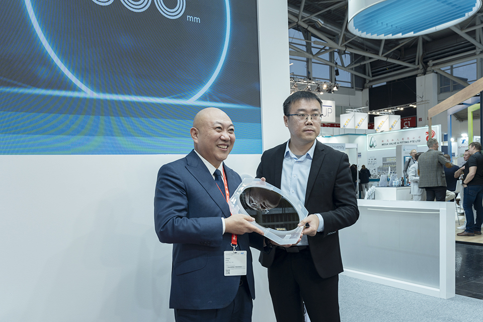
For the first time in the industry, SICC showcased a state-of-the-art 300mm silicon carbide substrate , which is the most advanced and largest diameter SiC substrate technology in the compound semiconductor industry. With this product, SICC has demonstrated the feasibility of its innovation and frontier technology.
SICC is the global qualified and high-reliable partner in the manufacturing of silicon carbide wafers. The company is currently further expanding its 200mm silicon carbide wafer manufacturing capacity in Shanghai .
About SICC Co., Ltd:
SICC is your global qualified partner in manufacturing of silicon carbide wafers. SICC provides multiple types of top-level quality silicon carbide substrates to accelerate the industry transition to a more efficient energy consumption and a sustainable future. We unleash the power of possibilities through hard work, collaboration and a passion for innovation. Learn more at www.xiaopimanhua.com.


